


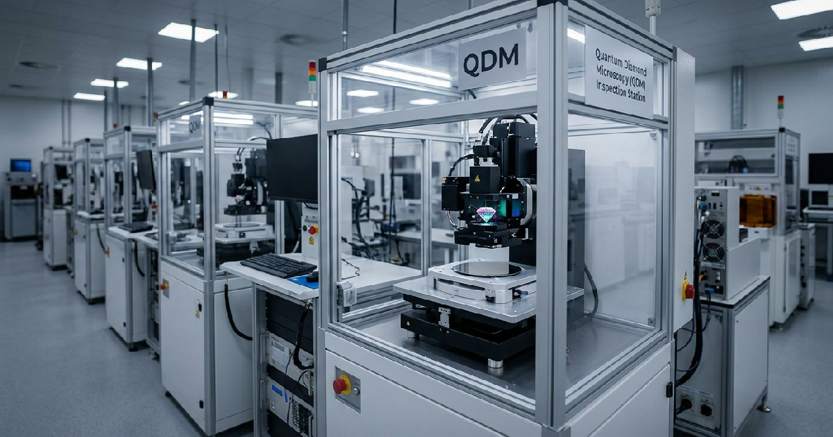
QuantumDiamonds has secured €91 million in fresh funding to scale its quantum-based semiconductor inspection technology, aiming to significantly accelerate chip manufacturing cycles.
The funding will support the construction of a new production facility in Munich, described by the company as the world’s first site for manufacturing semiconductor testing equipment based on quantum sensors. By utilizing Quantum Diamond Microscopy (QDM), the startup aims to reduce defect detection times from several weeks to just two minutes.
QuantumDiamonds secures million for quantum sensor factory
This capability is critical as the industry shifts toward complex 3D chip architectures for AI data centres, where traditional surface-level inspection tools often fail to identify buried faults across multiple layers.
At the heart of the QuantumDiamonds approach is the use of synthetic diamonds containing atomic-scale defects that react to magnetic fields with extreme sensitivity. These quantum sensors allow engineers to effectively see how electricity flows through an integrated circuit in three dimensions.
Unlike conventional scanning electron microscopes that only capture surface images, the QDM system provides a sub-surface view without destroying the chip during the process. This non-destructive testing helps maintain production yields in high-volume environments.
Current semiconductor inspection processes often require sample chips to be removed from the production line for destructive analysis in a laboratory setting. Kevin Berghoff, CEO and co-founder of QuantumDiamonds, notes that the firm targets a shift from lab-based sample testing to high-throughput quality control directly within the fabrication plant, or “fab.”
The company’s lab tool, the QDm.1, has already been deployed at Eurofins EAG Laboratories in Sunnyvale, California, as the startup expands its reach to global manufacturers.
Improving yields in the era of 3D semiconductors
As transistors reach their physical limits in terms of size, manufacturers have turned to vertical stacking to increase compute density. These multi-layered 3D chips present a unique challenge for quality assurance because defects can be hidden deep within the structure.
The inability to detect these issues early in the manufacturing process leads to lower yields and wasted materials, driving up the cost of high-end processors used in artificial intelligence.
The QuantumDiamonds technology addresses this by pinpointing the precise location and depth of defects. This helps manufacturers pivot to more agile production cycles, as they can diagnose process failures in real-time.
According to the company, saving even a small percentage of yield can equate to hundreds of millions of dollars for memory makers and foundries. The new Munich facility will host sensor production lines and cleanroom integration spaces designed to refine these high-throughput systems for future packaging requirements.
Strategic European investment under the IPF-ATEST project
The €76 million grant is part of a project dubbed “IPF-ATEST,” marking a significant milestone for the European Chips Act. This policy framework was designed to bolster Europe’s semiconductor supply chain and strengthen its role in the global market.
By backing a deep-tech spinout from the Technical University of Munich (TUM), the European Commission is signaling its intention to foster a homegrown ecosystem around chip testing and metrology, a field typically dominated by a handful of large-cap firms in the United States.
However, this state aid comes with specific requirements. QuantumDiamonds has committed to collaborating with academic institutions and opening parts of its facility to other high-tech startups and research laboratories. Furthermore, the German government will receive a share of the profits if the project’s returns exceed specific benchmarks.
This model ensures that public investment supports the scaling of an essential industrial technology while providing a potential return to the treasury. The startup’s current workforce of 70 is expected to grow, with plans to double the engineering team over the next 12 months.
Expanding the reach of German quantum engineering
While the manufacturing core remains in Bavaria, the company has aggressively pursued international markets throughout 2026. Setting up a regional hub in Taiwan was a strategic move to be closer to major memory makers and top-tier foundries. To date, QuantumDiamonds reports that it is already engaged with nine of the world’s ten largest semiconductor manufacturers, demonstrating significant industry pull for its quantum sensing tools.
The demand for such tools is global, and the company indicates a rapid return on investment despite the high cost of the equipment. While lab tools cost in the single-digit millions, high-throughput systems are expected to reach between $10 million and $15 million.
This international expansion mirrors the trajectory of other automated sectors, such as the cobot market which is expected to reach $2.18 billion by 2026 as manufacturers seek to automate precision tasks and improve plant agility.
Competition and the quest for domestic industrial leadership
Venture capital investors, including World Fund managing partner Daria Saharova, have suggested QuantumDiamonds could eventually become a success story similar to ASML. While ASML currently holds a near-monopoly on lithography machines, QuantumDiamonds is establishing a first-mover position in quantum-based inspection. Berghoff states that no U.S.
or Asian competitors have yet shipped similar tools to fabrication plants, giving the Munich startup a temporary advantage in the field.
Future growth will depend on the company’s ability to integrate its software and hardware seamlessly into the fast-paced environment of a modern fab. The startup charges a subscription fee for the software that interprets sensor data, providing a layer of recurring revenue alongside its hardware sales.
Much like the opening of advanced biotechnology facilities elsewhere, establishing a specialized production site in Munich creates a concentrated hub of expertise that is difficult to replicate quickly.
The final quarter of 2026 will be a proving ground for the startup as the first sections of the new Munich production facility become operational. If QuantumDiamonds can successfully deploy high-throughput 100% quality control, it could fundamentally change the economics of semiconductor fabrication.
By identifying process errors hours after they occur rather than weeks later, manufacturers can prevent the loss of thousands of wafers, securing the supply chain for next-generation computing.
