


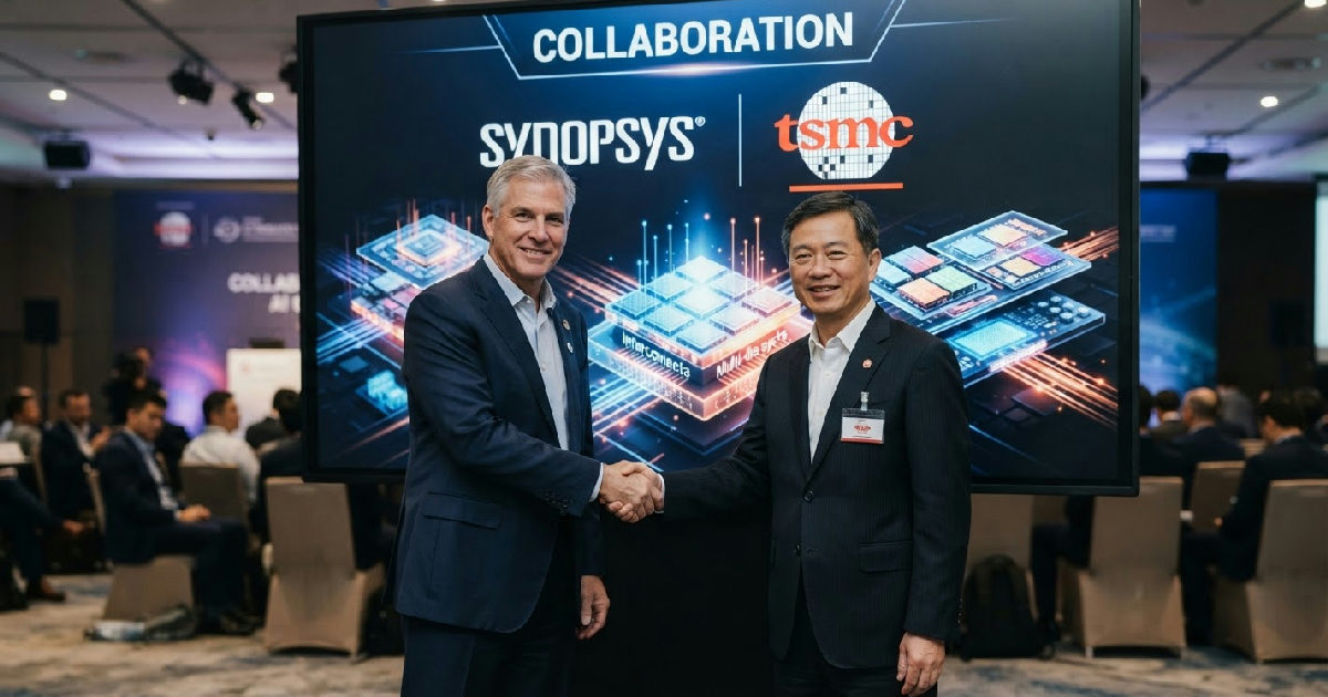
Synopsys and Taiwan Semiconductor Manufacturing Company (TSMC) have expanded their long-standing collaboration to support the development of next-generation artificial intelligence hardware.
The expanded partnership combines Synopsys’ AI-powered electronic design automation (EDA) software with TSMC’s advanced process and packaging technologies. The collaboration is intended to help customers manage increasing design complexity, improve energy efficiency and accelerate semiconductor development.
Synopsys-TSMC collaboration applies AI to semiconductor design
The collaboration spans several areas, including new design flows for TSMC’s A14 process node and silicon-proven IP for its 2nm technology.
A central element of the announcement is the use of AI in semiconductor design for future AI systems. Synopsys is integrating “agentic AI” capabilities across its digital and analogue design workflows.
This allows the software to automate highly complex tasks that have traditionally been bottlenecks for engineering teams, a problem familiar to those working on complex engineering projects like creating assistive device designs.
For example, Synopsys says its Custom Compiler™ tool uses AI to accelerate analogue design migration between process nodes. Its Fusion Compiler™ platform uses large language models (LLMs) to assist engineers with analysis and design tasks. These certified flows cover the process from implementation to final sign-off and are intended to support designers working with TSMC’s A14 technology.
According to Michael Buehler-Garcia, Senior Vice President at Synopsys, the scale and complexity of modern AI systems demand this level of integration. “Our joint innovations with TSMC address the continuum of silicon-to-systems co-design capabilities needed to accelerate development of next-generation AI and high-performance computing systems,” he stated.
The use of AI-assisted engineering is intended not only to reduce design time but also to support increasingly complex semiconductor designs. As transistor dimensions decrease and chip architectures become more complex, these tools can help designers meet power, performance and area (PPA) targets.
The tools can also allow chip architects to explore design options while automating parts of the implementation process.
Addressing multi-die design and packaging challenges
As chip designs become more complex, the industry is increasingly adopting multi-die systems. These designs, often called chiplets, combine multiple smaller, specialised chips within a single package. This approach can improve manufacturing yields and allows designers to combine technologies, but it also introduces packaging and integration challenges.
A significant part of the Synopsys-TSMC collaboration focuses on this area. The collaboration includes an agentic AI flow for chiplet floorplan co-optimisation using the Synopsys 3DIC Compiler platform. The flow is designed to automate chiplet floorplanning on advanced packages and supports TSMC’s 3DFabric® technologies for die-to-die connectivity.
The partners also highlighted a demonstration of die-to-die connectivity using the Universal Chiplet Interconnect Express (UCIe) standard. The demonstration used 32G/40G UCIe-A silicon on a TSMC N3P test chip integrated with a CoWoS-S interposer.
Synopsys has also completed 64G UCIe IP tape-outs on 2nm and 3nm process nodes, providing IP options for customers developing AI and high-performance computing systems.
Aveek Sarkar, Director of the Ecosystem and Alliance Management Division at TSMC, commented on the importance of this ecosystem approach. “By combining certified EDA solutions and a silicon-proven IP portfolio from Synopsys with our latest process and packaging innovations, we are enabling customers to push the boundaries of performance, integration, and energy efficiency,” Sarkar said.
Power and connectivity for next-generation systems
The increasing computational demands of AI models are driving higher power requirements for computing systems. Managing power consumption is therefore an important consideration in system design. The collaboration addresses this through better support for multi-die designs and the adoption of novel interconnect technologies.
Integrated voltage regulators and power efficiency
One critical innovation for managing power in complex packages is the use of integrated voltage regulators (IVRs). Instead of relying solely on larger off-package components, IVRs can be integrated closer to the chiplets they power. This can provide finer-grained voltage control and support faster responses to changes in power demand associated with AI workloads.
The Synopsys 3DIC Compiler platform now enables designers to co-design and simulate IVRs for systems using TSMC’s CoWoS® technology. This unified environment allows engineers to model thermal and electrical interactions between logic chips and IVRs and evaluate system behaviour under load. The capability is intended to support the design of high-power systems for AI and high-performance computing applications.
The rise of co-packaged optics
As data rates within servers and between components continue to climb, traditional copper interconnects can present bandwidth, distance and power-consumption constraints. Co-packaged optics (CPO) is an emerging technology that integrates optical communication components more closely with electronic devices. CPO can convert electrical signals to optical signals close to the processing hardware, potentially supporting higher bandwidth and lower power consumption in some applications.
Synopsys and TSMC are streamlining the development of these complex systems. Their joint enablement for TSMC-COUPE™ technology provides an integrated photonic and electronic co-design flow. This allows engineering teams to handle optical path simulation, electromagnetic analysis, and system-level verification within a single, coherent workflow, supporting the development of optical interconnects for future HPC and AI architectures.
Silicon-proven IP for advanced process nodes
Beyond design tools, the collaboration includes a portfolio of pre-verified IP blocks. The silicon-proven IP provides pre-designed circuits for common interfaces, which can reduce development work and associated design risks. Instead of designing an interface such as PCIe from scratch, customers can license Synopsys IP that has been validated for use on supported TSMC process technologies.
The partners also announced IP milestones for TSMC’s N2P process, a further development of the foundry’s 2nm technology. The IP portfolio ready for AI and HPC designs includes solutions for PCIe 7.0, HBM4 high-bandwidth memory, LPDDR6/5X/5 memory, and 224G Ethernet PHYs. These components support connectivity between processors, memory, accelerators and networks in AI and high-performance computing systems.
The portfolio also extends to automotive applications, with Synopsys offering a UCIe IP solution compliant with ASIL B functional safety requirements on TSMC’s N5A process. The IP is intended to support chiplet-based designs for automotive applications requiring ASIL B functional-safety compliance.
The IP portfolio spans process nodes from 6nm to 2nm and covers applications including data centres, mobile devices, automotive systems and edge AI.
