


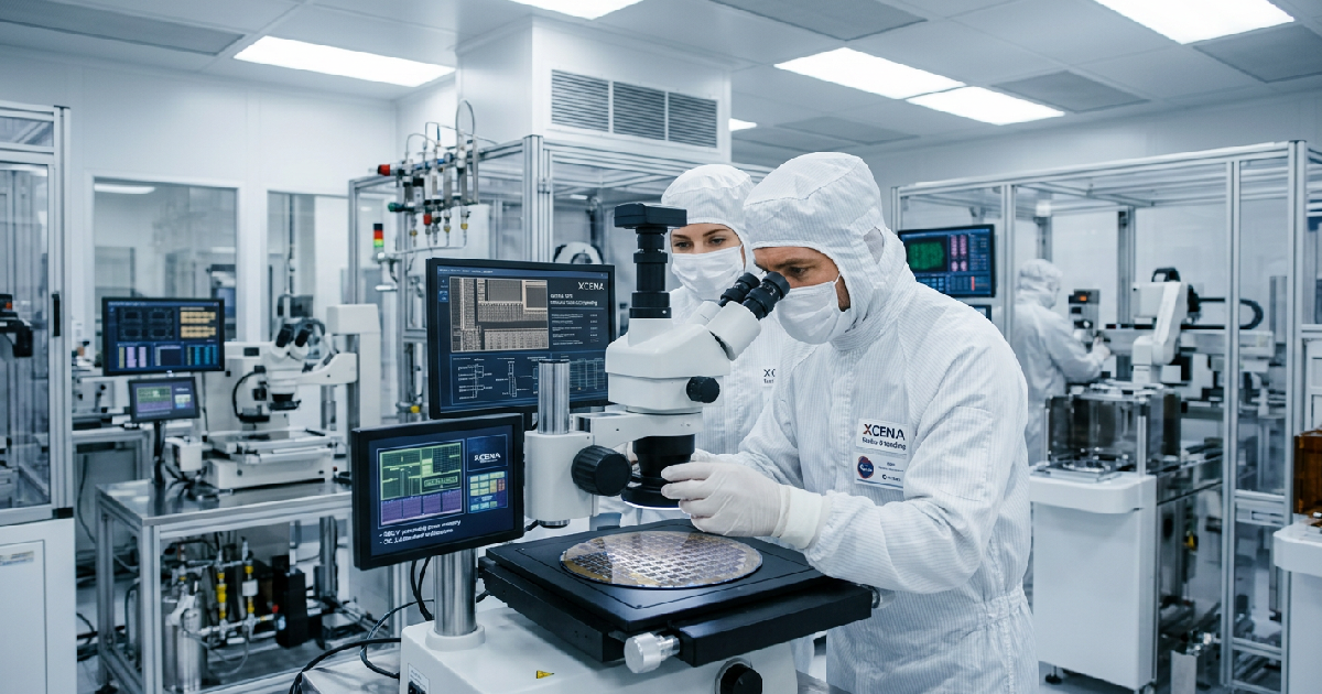
Semiconductor startup XCENA has secured $135 million in Series B funding to scale the production of its MX1 computational memory chip, an engineering solution designed to eliminate the data bottlenecks hindering large-scale artificial intelligence (AI) systems. The financing round, announced on May 29, 2026, was co-led by Seoul-based venture firms Atinum Investment and IMM Investment, bringing the company’s total capital raised to $185 million. With a post-money valuation of $570 million, the startup plans to initiate mass commercial production on Samsung foundry lines by the end of 2026.
The investment addresses a critical shift in industrial computing as the “memory wall”—the physical limit of how fast data moves between a processor and its storage—becomes a tighter constraint than raw processing power. XCENA’s leadership team, including CEO Jin Kim, CTO Dohun Kim, and CPO Harry Juhyun Kim, includes veterans from Samsung Electronics and SK Hynix. They founded the company in 2022 to challenge traditional von Neumann architecture, where data is stored in one place and worked on elsewhere.
For high-intensity generative AI, this constant physical separation drives up latency and energy expenditure.
By integrating large memory arrays directly with computational resources, XCENA intends to reduce the infrastructure footprint of modern data centres. Preliminary metrics show that certain AI workloads that typically require approximately 10 servers can run on a single server equipped with MX1 hardware. This density improvement is central to the rally seen in industrial and engineering stocks recently, as investors look for hardware that can process data in-situ rather than moving it across slow links.
Engineering the MX1 computational memory architecture
The MX1 chip serves as a computational memory controller that merges high-capacity pooled DDR5 memory with thousands of proprietary 64-bit RISC-V processing cores. Unlike standard memory modules that merely store bits, the MX1 performs active tasks like key-value (KV) cache management and data preprocessing within the memory module itself. This architecture is built on the open Compute Express Link (CXL 3.x) standard, which supports cache-coherent communication between host processors and memory expansion devices.
Engineers at XCENA designed the MX1 to support up to 2TB of DDR5 memory per unit. A feature dubbed InfiniteMemory™ further extends this capacity to petabyte-scale by using SSDs with minimal latency penalties. This scale is vital for modern large language models that face KV cache overflow during long-context inference. “AI workloads are exposing the fundamental limitations of traditional computing architectures,” said Jin Kim, CEO of XCENA, noting that expanding context windows are driving unprecedented memory demands.
To support rapid integration, the company provides a full-stack software development kit (SDK) called XFLARE. This toolset enables research institutions and enterprise customers to migrate existing workflows onto XCENA hardware without extensive software rewrites. Such advancements in global developer relations and engineering support are becoming essential as hardware complexity increases, requiring more sophisticated APIs for industrial implementation.
Production timeline and market growth projections
XCENA operates on a fabless silicon design model, focusing internal resources on R&D centres in Sunnyvale, California, and Banqiao, South Korea. The startup has scheduled mass production on Samsung’s 4-nanometer foundry lines for late 2026. Working samples of the MX1P model are slated for delivery to select partners in October 2025, followed by the more advanced MX1S model in 2026. Initial revenue is expected to follow in 2027.
The commercial opportunity for CXL-compliant hardware is expanding at pace. Industry projections suggest the CXL component market could grow from approximately $700 million in 2025 to $16 billion by 2028. XCENA enters this space alongside established players like Marvell and Astera Labs, but its specific focus on near-data processing (NDP) for AI inference provides a distinct engineering angle. In benchmarks, the MX1 has demonstrated up to a 3.9x improvement in time-to-first-token for AI inference.
The impact of this hardware is being felt across the engineering sector as firms look to simplify complex infrastructure. While some regions focus on software, others are seeing new engineering initiatives that prioritise the physical hardware required to sustain productivity. As XCENA expands its presence in Northern California to work with hyperscale cloud providers, the focus remains on eliminating the inefficiencies that have traditionally slowed down advanced computing workflows.
Strategic significance for industrial AI infrastructure
The Series B syndicate included several Asian institutional investors, such as SBI Investment, Mirae Asset Capital, Corstone Asia, and the Korea Development Bank. This collective backing indicates a strong belief that the future of industrial productivity lies in hardware that can process data “where it sits.” For many operations managers, the ability to consolidate server racks translates directly into lower cooling costs and reduced power requirements per computational unit.
XCENA is betting that the industry will continue to move away from discrete, siloed components toward a more integrated memory-centric model. As mass production nears, the true test will be how effectively the MX1 integrates into the existing hyperscale ecosystems of global cloud providers. If the startup hits its production targets for late 2026, it may provide the hardware roadmap needed to sustain AI development without crashing into the physical limits of current memory architecture.
