


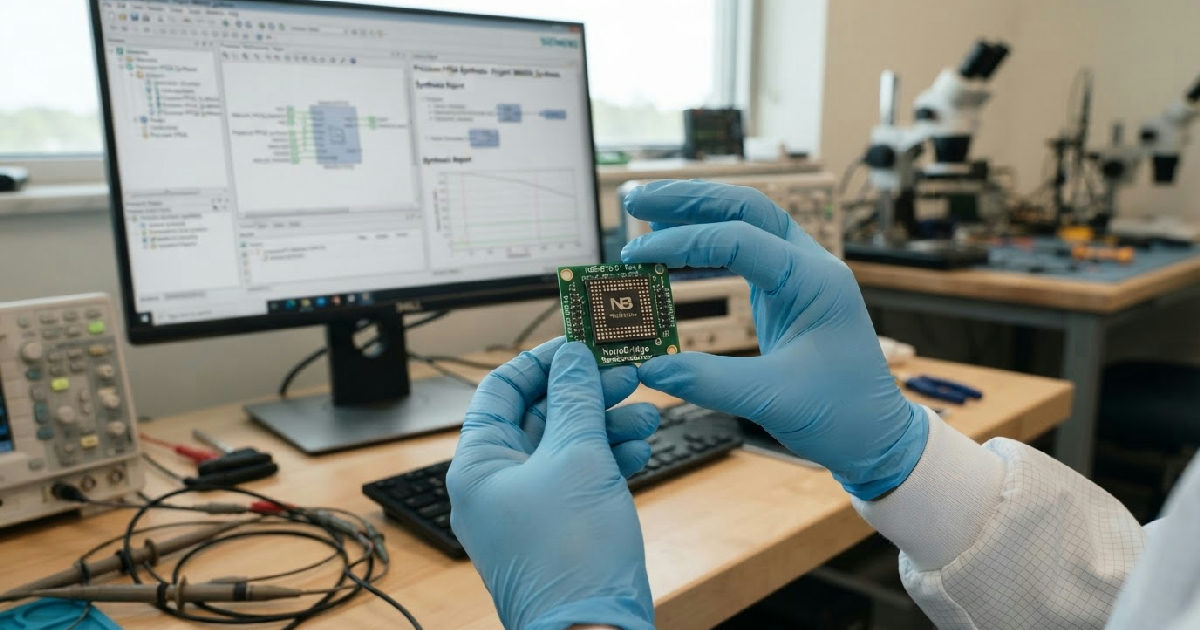
NanoBridge Semiconductor Inc. will use a new Siemens FPGA synthesis tool for its low-power industrial chips. will use a new Siemens FPGA synthesis tool for its low-power industrial chips.
Announced on September 3, 2026, the deal involves an original equipment manufacturer (OEM) agreement. NanoBridge will provide its customers with a version of Siemens’ Precision FPGA Synthesis software specifically configured for its own device families. This simplifies the complex process of turning high-level hardware description language designs into optimised silicon.
A tailored design flow for NanoBridge Siemens FPGA synthesis
This collaboration extends beyond a simple software licence. It establishes a finely tuned synthesis and implementation workflow for NanoBridge’s NBS6503H and NBS1201 field-programmable gate array (FPGA) families. For hardware developers, this means a smoother, more efficient path from concept to a functioning chip, backed by a supported ecosystem that reduces integration headaches.
A core challenge with any specialised semiconductor is ensuring that design tools can fully exploit its unique features. The Siemens software platform will be calibrated to understand the specific routing and logic block configuration of NanoBridge’s non-volatile architecture.
This integrated software maps high-level hardware description languages into an optimised gate-level netlist, ensuring the automated process makes the most efficient use of the silicon.
Such deep integration is vital for achieving high-quality synthesis results and efficient implementation workflows in advanced semiconductor development, reflecting broader trends in Nvidia’s AI infrastructure and other complex industrial computing solutions.
Yukio Tsuchida, Vice President for Siemens EDA in Japan, framed the partnership as a way to empower innovation. “Our collaboration with NanoBridge Semiconductor… demonstrates how Siemens’ technology can help semiconductor innovators accelerate development, reduce complexity and bring advanced products to market with confidence,” he said. The goal is to give developers a competitive edge by lowering the barrier to using this advanced programmable logic.
What is NanoBridge’s atomic switch technology?
At the heart of NanoBridge’s FPGAs is its proprietary atomic switch technology. Unlike conventional FPGAs that use static RAM (SRAM) to configure logic, NanoBridge employs a non-volatile switch. This component functions by creating and breaking a metal bridge at the nanoscopic level within the semiconductor chip, directly controlling the metal wiring.
This fundamental difference in architecture delivers significant advantages. The company reports that its FPGAs can achieve power savings of up to 90% and offer approximately ten times the power efficiency compared to their conventional counterparts. In some cases, the technology can reduce power consumption to just one-quarter across the entire chip.
This efficiency stems from a smaller chip area, shorter internal wiring, and lower operating voltages, contributing to higher speeds and greater reliability.
Because the configuration is non-volatile, the chip retains its state even when powered down, eliminating the need for an external boot device. This not only saves board space and cost but also improves system reliability and security, particularly in environments where power cycles may be frequent or unpredictable. The technology exemplifies how hardware innovation underpins the move towards more complex, energy-efficient systems.
Targeting the toughest industrial and automotive applications
The primary markets for this technology are sectors where failure is not an option and power efficiency is paramount. NanoBridge specifically targets aerospace, smart infrastructure, secure elements for data protection, and automotive systems. In these applications, the ability to operate reliably in extreme temperatures, high-vibration settings, or with limited power budgets is a critical design requirement for control units and sensing platforms.
For example, a sensor package on an aircraft wing or an engine control unit in a vehicle must be completely dependable, often operating without easy access for maintenance. The non-volatile nature and extreme power efficiency of NanoBridge’s FPGAs make them an ideal fit for such demanding scenarios.
The partnership with Siemens is designed to streamline the process for engineers in these highly regulated industries to adopt and validate the technology for their specific use cases, much like how VI-grade simulator integrated into automotive development enhances component testing.
Toshitsugu Sakamoto, Co-founder and Chief Technology Officer at NanoBridge, highlighted this focus. “NanoBridge Semiconductor is focused on advancing low-power and harsh-environment semiconductor technologies for aerospace, automotive and critical infrastructure,” he stated. “Our adoption of Siemens’ Precision FPGA Synthesis enables us to provide our customers with a synthesis flow tailored for our FPGA device families while continuing to expand the ecosystem supporting our technologies.”
A boost for edge computing
The operational benefits extend directly to the burgeoning field of edge computing. As more data processing shifts from centralised data centres to devices at the network’s edge—from factory floors to remote agricultural sensors—power consumption becomes a primary limiting factor. Devices that can perform complex tasks without being tethered to a constant, high-capacity power source are essential.
The power efficiency of NanoBridge’s FPGAs could enable more sophisticated processing in battery-powered or energy-harvesting devices. This could accelerate the deployment of intelligent sensors and controllers in locations previously considered impractical, contributing to trends like AI-driven maintenance where on-device analysis is key.
Wider implications for semiconductor design
This OEM agreement reflects a broader industry trend toward deeper collaboration between electronic design automation (EDA) software providers and specialised chip makers. By delivering a pre-optimised toolchain, the partnership removes a significant barrier for smaller engineering teams who may lack the resources to fine-tune generic tools for a niche architecture.
For developers, the practical benefits are clear: reduced compilation times during the design phase, lower power consumption in the final manufactured circuit, and increased stability during the crucial hardware verification stage. This allows them to focus more on the application-level challenges rather than the intricacies of low-level hardware implementation.
The collaboration aims to accelerate innovation and broaden the adoption of NanoBridge’s FPGA solutions for what Sakamoto calls “some of the world’s most demanding applications and environments.”
